Huawei Claims LogicFolding Architecture Achieves 1.4nm-Class Density Without EUV, Targets 2031 Production
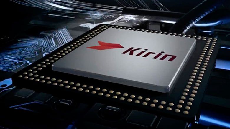
The timing matters: Huawei's announcement follows two weeks of successful sanctions workarounds (die-on-board NAND packaging, new chip design methodology) and arrives as the U.S. is negotiating Iran sanctions relief and signaling openness to strategic dealmaking.
If this is credible, it shifts the calculus for BIS export control policy — the agencies can no longer assume process-node restrictions alone will constrain Chinese capability. Conversely, if LogicFolding is vaporware, it's a public relations move designed to signal to Beijing that Huawei is fighting back, which has domestic political value even if the tech doesn't ship.
The real test is whether Chinese foundries (SMIC, CXMT) can license or reverse-engineer the approach by 2028.
If Huawei's claims are validated in silicon, it signals a viable path for Chinese semiconductor firms to close the process-node gap without EUV access — directly undermining the premise of U.S. export controls that assume advanced nodes are unreachable without Western equipment.
The Commerce Department's EUV export ban has been the binding constraint on China's domestic chip capability; a credible workaround collapses that leverage. Watch whether TSMC, Samsung, or independent foundries can replicate or validate LogicFolding's density claims by mid-2027 — that's when the claim either holds up or evaporates.
Has Huawei demonstrated LogicFolding on actual silicon, or is this a design-stage announcement? The article cites claims but no tape-out, test results, or third-party verification. What specific node (28nm, 14nm, 7nm?) is Huawei using to prototype LogicFolding?
Fault Lines
Strategic intelligence, synthesized daily — with a public track record. Every call graded against what actually happened.