IBM Spins Off Quantum Foundry With $2B Federal-Private Funding; Anderon Targets 300mm Wafer Capacity
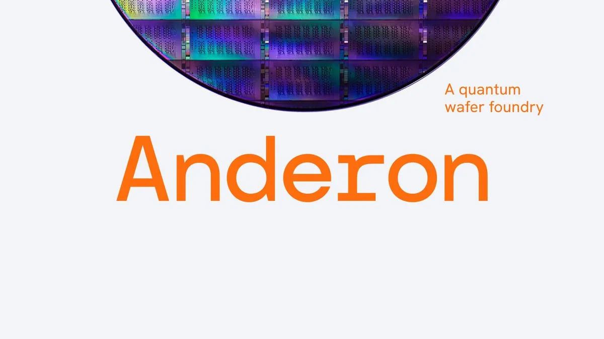
The foundry model works only if yield economics improve faster than quantum device complexity grows. If Anderon can't achieve 40%+ yields on advanced nodes within 24 months, the 300mm fab becomes a $2B stranded asset. The real constraint is customer lock-in: Anderon must convince quantum hardware startups (IonQ, Rigetti, D-Wave, and others) to trust a third party with proprietary designs.
IBM's own quantum division is now a competitor to its former captive customers — that structural conflict will surface in pricing negotiations and technology roadmap disputes.
This is the first U.S. attempt to create a dedicated quantum foundry model — separating chip design from manufacturing to enable third-party access.
The 300mm fab footprint signals a bet that quantum device yields and volumes will reach commercial manufacturing scale within 3-5 years; if that timeline slips, the capital intensity becomes a liability for both Anderon and its federal backers.
Watch whether the Commerce Department or DARPA issues guidance on export controls for quantum foundry services — quantum computing sits at the intersection of dual-use AI infrastructure and national security, and foundry access is a leverage point Beijing will target.
What is the actual breakdown of the $2B between federal and private capital? The article doesn't specify how much came from government (CHIPS Act, DARPA, NSF, or other) versus venture/corporate investors — that split determines whether Anderon operates as a subsidy-dependent incumbent or a market-dr...
Fault Lines
Strategic intelligence, synthesized daily — with a public track record. Every call graded against what actually happened.