Google Books Intel for 3M+ TPU Packaging in 2028; SK Hynix Tests EMIB for HBM
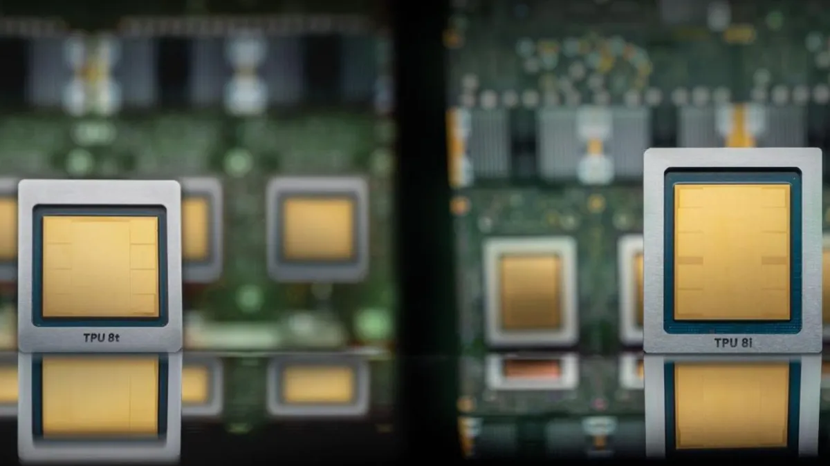
If Intel successfully qualifies EMIB with SK Hynix, the packaging layer becomes a new competitive front in AI chip design — one where TSMC has no inherent advantage and where Intel's process legacy (advanced interconnect design) is actually an asset.
This opens a second revenue channel for Intel's foundry division: packaging-only contracts from fabless designers and memory makers who want chiplet integration without committing to a single process node. The risk: if yields or costs don't match TSMC's packaging economics, Google's 2028 ramp could become a sunk-cost anchor dragging down Intel's unit economics.
Intel has locked a major customer for a critical AI infrastructure component through 2028, validating its advanced packaging as a viable alternative to TSMC for chiplet assembly — and signaling that Intel's foundry ambitions extend beyond process nodes into the high-margin packaging layer.
Google's 3M-unit commitment is a $1.5B+ revenue stream (at estimated $500+ per packaged unit) that Intel needs to stabilize its foundry division, which has bled customers since 2023.
The EMIB testing by SK Hynix suggests Intel is positioning packaging as a standalone competitive moat: if Hynix qualifies EMIB for HBM stacks, Intel moves from foundry vendor to critical infrastructure partner for memory-compute integration across the industry. Watch whether TSMC responds with packaging acceleration or whether Nvidia and AMD commit to Intel packaging for next-generation designs.
Does the Google order include penalty clauses for yield or delivery delays, and what is Intel's actual packaging capacity utilization in 2027-2028 before this ramp?
Fault Lines
Strategic intelligence, synthesized daily — with a public track record. Every call graded against what actually happened.